この商品を友人に教える:
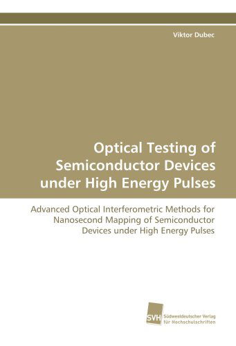
Optical Testing of Semiconductor Devices Under High Energy Pulses: Advanced Optical Interferometric Methods for Nanosecond Mapping of Semiconductor Devices Under High Energy Pulses Viktor Dubec
価格
¥ 9.956
税抜
遠隔倉庫からの取り寄せ
発送予定日 年11月23日 - 年12月3日
 クリスマスプレゼントは1月31日まで返品可能です

Viktor Dubec の新しいリリースのお知らせを受け取る


iMusicのウィッシュリストに追加
Optical Testing of Semiconductor Devices Under High Energy Pulses: Advanced Optical Interferometric Methods for Nanosecond Mapping of Semiconductor Devices Under High Energy Pulses
Viktor Dubec
For optimisation of devices and verification of device simulation models the knowledge of heat dissipation and of free carrier concentration in the device is essential. Non-destructive optical methods based on monitoring of the refractive index, absorption or light emission have previously been developed for investigation of transient temperature or free carrier changes. However, these methods suffer either from small spatial or time resolution. Therefore two testing techniques based on transient interferometric mapping have been developed within this thesis: a two-dimensional multiple-time-instant single-shot technique and a two-beam technique with sub-nanosecond time resolution.
| メディア | 書籍 Paperback Book (ソフトカバーで背表紙を接着した本) |
| リリース済み | 2009年3月3日 |
| ISBN13 | 9783838104041 |
| 出版社 | Suedwestdeutscher Verlag fuer Hochschuls |
| ページ数 | 160 |
| 寸法 | 150 × 220 × 10 mm · 256 g |
| 言語 | ドイツ語 |


